|
|
- 武部 幹,岩田 穆,高橋宣明,国枝博昭共著,
スイッチトキャパシタ回路, 現代工学社(1985)
- 楠 菊信,岩田 穆,赤沢幸雄著,
VLSIのためのアナログ技術,共立出版,(1989)
- 加藤浩太郎,岩田 穆他著, LSI技術の基礎,電気通信協会 (1992)
- 岩田 穆他共著, LSIハンドブック,電子情報通信学会,(1984)
- 岩田 穆,雨宮好仁,藤田 修,内村国治,森江 隆共著,
ニューラルネットワークLSI,電子情報通信学会
- 岩田穆,桜井康貴他(分担執筆)低消費電力,高速LSI技術,リアライズ社,(1997)
- 岩田穆,森江隆,永田真 他(分担執筆)
CMOSアナログ回路設計技術(岩田穆 監修),トリケップス社,1998
- 岩田 穆著, CMOS集積回路の基礎
(集積回路入門教科書)科学技術出版,2000
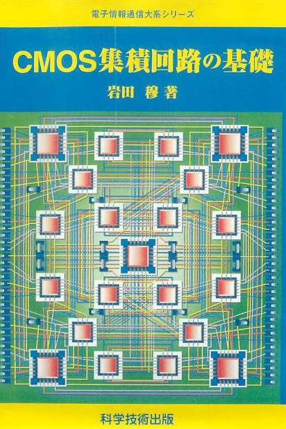
論理回路,メモリ,アナログ回路の
機能,デバイス,回路,特性,設計について解説
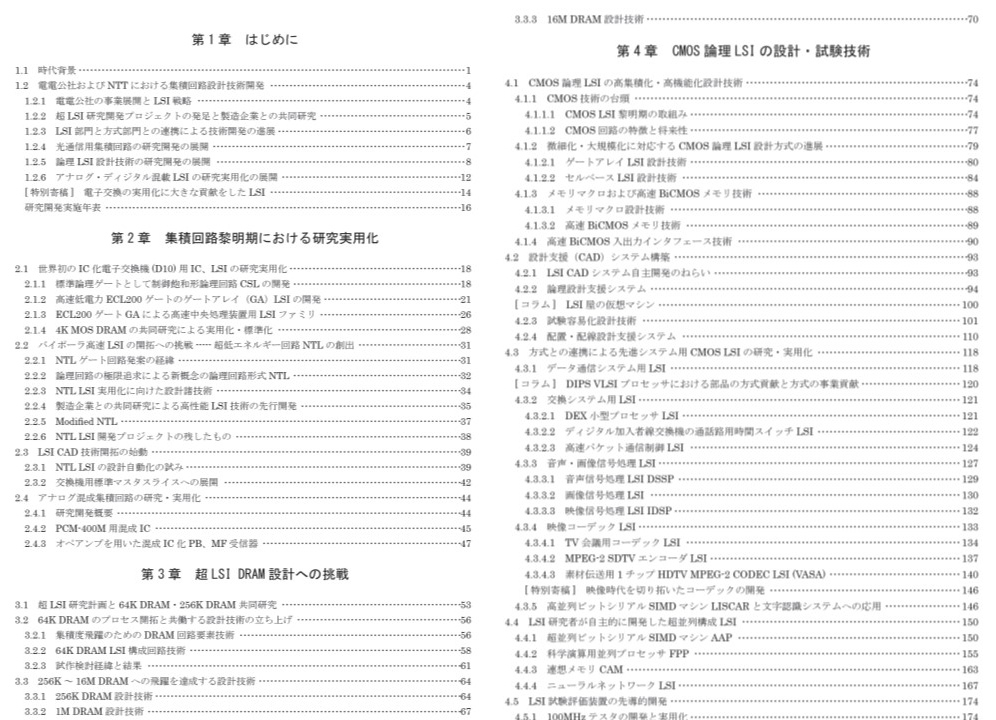
第1章:イントロ
第2章:デバイス
第3章:CMOSプロセス
第4章:CMOS論理回路
第5章:遅延時間・消費電力
第6章:半導体メモリ
第7章:演算回路
第8章:制御回路
第9章:アナログ回路
第10章:AD変換器
第11章:フィルタ
第12章:・EEン計技術
初版の正誤表, 2刷の正誤表
- 岩田 穆著, VLSI工学-基礎・設計編- 電子情報通信学会レクチャーシリーズ、
(平成18年 コロナ社)
中国語訳本 
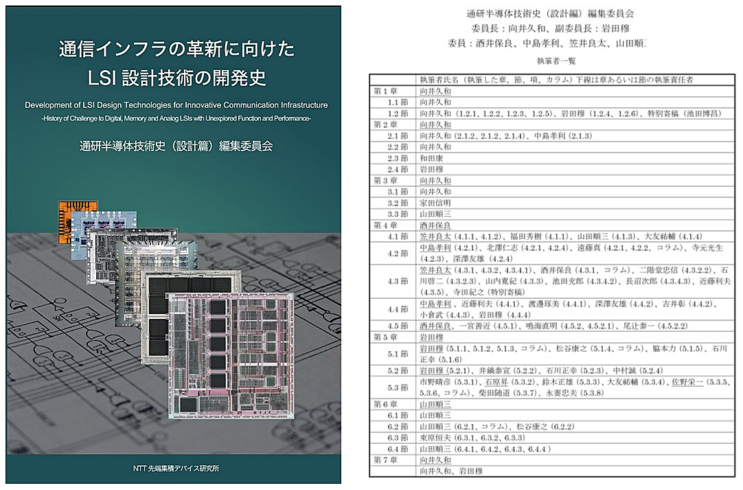
- 向井久和編集委員長 岩田編集副委員長
「通信インフラの革新に向けたLSI設計技術の開発史」 2018年12月
NTT 先端集積デバイス研究所 制作 非売品
--目次--
- 岩田 穆,吉村 寛,柳川文彦
多周波受信器用混成集積化RCアクティブBPFの設計
信学論(C), Vol. 60-C, No. 6, pp. 359-366, (1977) - 岩田 穆,中山 了,斉藤保直,丹生和男
レーザによる混成IC化RCアクティブフィルタの機能トリミング
信学論(C), Vol. 60-C, No. 11, pp. 669-675, (1977) - Goichi Tatsuno, Minpei Fujinami, Atsushi Iwata and Kaoru Kinamari
Precision Electron Beam Exposure System, EB-52
Revue de Physique Appliquee, Vol. 13, pp. 705-708, (1978) - Atsushi Iwata, Kuniharu Uchimura, Sanshiro Hattori, Hiroaki Shimizu and Kazuo Ogasawara
Low Power PCM CODEC and Filter System,
IEEE J. of Solid-State Circuits, Vol. SC-16, No. 2, pp. 73-79, (1981) - Atsushi Iwata, Hiroyuki Kikuchi, Kuniharu Uchimura, Akihiko Morino and Masahiko Nakajima,
A Single-chip CODEC with Switched-Capacitor Filters,
IEEE J. of Solid-State Circuits, Vol. SC-16, No. 4, pp. 315-321, (1981) - Yukio Akazawa, Yasuyuki Matsuya and Atsushi Iwata,
New Linearity Error Correction Technology for A/D and D/A Converter LSI,
JJAP,Vol. 22, Sup.22-1, pp. 115-119, (1983) - Kazunari Irie, Takehiko Uno, Kuniharu Uchimura and Atsushi Iwata,
A Single-chip ADM LSI CODEC,
IEEE J. of Solid-State Circuits, Vol. SC-18, No. 1, pp. 33-39, (1983) - Yukio Akazawa, Hiroyuki Kikuchi, Atsushi Iwata, Takashi Matuura and Toru Takahashi,
Low Power 1 GHz Frequency Synthesizer LSIs,
IEEE J. of Solid-State Circuits, Vol. SC-18, No. 1, pp. 115-121, (1983) - 金子孝夫,菊池博行,岩田 穆,
多重化スイッチトキャパシタフィルタの設計法,
信学論(C), Vol. J67-C, No. 7, pp. 588-595, (1984) - 松谷康之,赤沢幸雄,岩田 穆, 高精度,高速CMOS1チップA/D,D/A変換器-全デジタル精度補正法 (LECS),
信学論 (C), Vol. J69-C, No. 5, pp. 531-539, (1986) - Junichi Takahashi, Takashi Kimura, Sanshiro Hattori and Atsushi Iwata,
A Ring Array Processor Architecture for Highly Parallel Dynamic Time Warping,
IEEE Trans. ASSP, Vol. 34, No. 5, pp. 1310-1318, (1986) - Yasuyuki Matsuya, Kuniharu Uchimura and Atsushi Iwata,
A 16-bit Oversampling A-to-D Conversion Technology Using Triple-Integration Noise Shaping,
IEEE J. of Solid-State Circuits, Vol. SC-22, No. 6, pp. 921-929, (1987) - Kuniharu Uchimura, Toshio Hayashi, Tadakatsu Kimura and Atsushi Iwata,
Oversampling A-to-D and D-to-A Converters with Multi-stage Noise Shaping Modulators,
IEEE Trans. ASSP, Vol. 36, No. 12, pp. 1899-1905, (1988) - Eiichi Sano, Tuneo Tsukahara and Atsushi Iwata,
Performance Limits of Mixed Analog/digital Circuits with Scaled MOSFETs,
IEEE J. of Solid-State Circuits, Vol. SC-23, No. 4, pp. 942-949, (1988) - Kenji Nakayama, Atsushi Iwata and Takeshi Yanagisawa,
(Invited) Present and Future Trends in Integrated Analog Signal Processing Circuits,
IEICE Trans. Vol. E71, No. 12, pp. 1177-1188, (1988) - 金子孝夫,山内寛紀,岩田 穆.
正規化浮動少数点VLSIシグナルプロセッサ:DSSP1
信学論 (B),Vol. J72-B-I, No. 1, pp. 67-73, (1989) - Yasuyuki Matsuya, Kuniharu Uchimura, Atsushi Iwata andTakao Kaneko,
A 17-bit Oversampling D-to-A Conversion Technology using Multistage Noise Shaping,
IEEE J. of Solid-State Circuits, Vol. SC-24, No. 4, pp. 969-975, (1989) - 岩田 穆,松谷康之,
オーディオ用1ビットAD, DA変換技術(1)
JAS Journal, Vol, 29, No.1, pp15-21, 1989. - 岩田 穆,松谷康之,
オーディオ用1ビットAD, DA変換技術(2)
JAS Journal, Vol, 29, No.2, pp.33-39, 1989. - Tadao Nagatsuma, Tsugumichi Shibata, Eiichi Sano and Atsushi Iwata,
Subpicosecond Sampling using a Noncontact Electro-optic Probe,
J. Appl. Phys. Vol. 66, No. 9, pp. 4001-4009, (1989) - Eiichi Sano, Tadao Nagatsuma, Tsugumichi Shibata and Atsushi Iwata,
Generation of Picosecond Electrical Pulses by Pulse-forming Optoelectronic Device,
Appl. Phys. Lett., Vol. 55, No. 2, pp.151-152, (1989) - M. Koga, T. Matsumoto, Y. Amemiya, A. Iwata and H. Miyao,
High-Speed Analogue Neural-Network LSI Employing Super-Selfaligned Si Bipolar Process Technology,
Electronics. Lett.,Vol. 27, No. 18, pp. 1678-1679, (1991) - O. Fujita, Y. Amemiya and A. Iwata,
Characteristics of Floating Gate Device as Analogue Memory for Neural Networks,
Electron. Lett., Vol. 27, No. 11, pp. 924-925, (1991) - T. Watanabe, T. Morosawa, N.. Shimazu, H. Morita, H. Yamauchi and A. Iwata,
Reliability Enhancements for the Direct Wafer Exposure Electron Beam System EB60,
J. of Vac. Sci. Technology B Vol.9, No.6, pp. 3028-3032, (1991) - H. Yamauchi, T. Morosawa, T. Watanabe and A.i Iwata,
Real-Time Feed- Forward Control LSIs for a Direct Wafer Exposure Electron Beam System,
IEICE Trans. Electron. Vol. E76-C, No. 1, pp. 124-135, (1993) - A. Iwata and I. Hayashi,
Optical Interconnections as a New LSI Technology,
IEICE Trans. Electron. Vol. E76-C, No. 1, pp. 90-99, (1993) - A. Iwata,
Optical Interconnection for ULSI Techmology Innovation,
Optoelectronics -device and Technologies, Vol. 9, No.1, pp.39-54, (1994) - A. Iwata and M. Nagata,
A Concept of Analog-Digital merged Circuit Architecture for Future VLSI's,
IEICE Trans. Fundamentals of Electronics, Communications and Computer Sciences,
Vol. E79-A, No.2, pp.145-157, (1996). - T. Doi, T. Namba, A. Uehara, M. Nagata, S. Miyazaki, K. Sibahara, S. Yokoyama, A. Iwata, T. Ae and M. Hirose,
Optically Interconnected Kohonen Net for Pattern Recognition,
JJAP, Vol.35. Part I, No. 2B, pp. 1405-1409 (1996) - T. Namba, A. Uehara, T. Doi, T. Nagata, Y. Kuroda, S. Miyazaki, K. Sibahara, S. Yokoyama, A .Iwata and M. Hirose,
High-Efficiency Micromirrors and Branched Optical Waveguides on Si Chips,
JJAP, Vol.35. Part I, No. 2B, pp. 941-945 (1996) - A. Iwata and M. Nagata,
A Concept of Analog-Digital merged Circuit Architecture for Future VLSI's,
Analog Integrated Circuits and Signal Processing, Vol.11, No.2, pp.83-96, (1996). - T. Doi, A. Iwata and M. Hirose,
Analysis and Design of Low Loss and Low Mode-Shift Integrated Optical Waveguides
Using Finite-Difference Time-Domain Method,
IEICE Trans. Electronics, Vol. E80-C, No.5, pp.625-631, (1997). - T. Morie, S. Sakabayashi, M. Nagata and A. Iwata,
Nonlinear function generators and Chaotic sugnal generators using a pulse-width modulation method,
Electronics letters, Vol.33, No. 16, pp.1351-1352, 31, July, 1997. - M. Saen, T. Morie, M. Nagata and A. Iwata,
A Stochastic Associative Memory using Single-Electron Tunneling Devices,
IEICE Trans. Electronics, Vol. E81-C, No.1, pp.30-35, 1998. - M. Nagata, J. Funakoshi and A. Iwata,
A PWM Signal Processing Core Circuit Based on a Switched Current Integration Technique,
IEEE Journal of Solid-State Circuits, Vol.33, No.1, pp.53-59, 1998. - T. Doi, A. Uehara, Y. Takahashi, S. Yokoyama, A. Iwata and M. Hirose,
An Experimental Pattern Recognition System Using Bidirectional Optical Bus Lines,
Jap. J. Appl. Phys., Vol. 37, Part I, No. 3B, pp.1116-1121, (1998). - M. Nagata and A. Iwata,
PWM Signal Processing Architecture for Intelligent Systems,
Computers & Electrical Engineering, Vol. 23, No. 6, pp.393-405, 1997 - 岩田,永田,森江,
アナログ・デジタル融合回路による知能処理LSI,
電子情報通信学会誌,Vol. 81, No. 9, pp.893-897, 1998. - 雨宮,岩田,広瀬,
単電子回路による知能集積デバイスの可能性,
電子情報通信学会誌,Vol. 81, No. 9, pp.898-902, 1998. - M. Nagata and A. Iwata,
Substrate Noise Simulation Techniques for Analog-Digital Mixed LSI Design (Invited)
IEICE Trans. Fundamentals, Vol. E82-A, No.2, pp.271-278, 1999. - T. Morie, J. Funakoshi, M. Nagata and A. Iwata,
An Analog-Digital Merged Neural Circuit Using Pulse Width Modulation Technique,
IEICE Trans. Fundamentals, Vol. E82-A, No.2, pp.356-363, 1999. - a. Iwata, N. Sakimura, M. Nagata and T. Morie,
The Architecture of Delta Sigma, Analog-to-Digital Converter using Voltage-Controlled Oscillator
as a Multibit Quantizer,
IEEE Trans. Circuits and Systems-II, Vol. 46, No.7, pp.941-945, 1999. - S. Kinoshita, T. Morie, M. Nagata and A. Iwata,
New Non-Volatile Analog Memory Circuits Using PWM Methods,
IEICE Trans. Electron., Vol. E82-C, No. 9, pp. 1655-1661, 1999. - T. Morie, K. Uchimura, Y. Amemiya,
Analog LSI Implementation of Self-Learning Neural Networks,
Computers and Electrical Engineering, Vol. 25, No. 5, pp. 339-355, 1999. - H. Ando, T. Morie, M. Nagata and A. Iwata,
A Nonlinear Oscillator Network for Gray-level Image Segmentation and PWM/PPM Circuits
for its VLSI Implementation,
IEICE Trans. Fundamentals, Vol. E83-A, No. 2, pp. 329-336, 2000. - T. Morie, T. Matsuura, S. Miyata, T. Yamanaka, M. Nagata and A. Iwata,
Quantum Dot Structures Measuring Hamming Distance for Associative Memories,
Superlattices and Microstructures, Vol. 27, No. 5/6, pp. 613-616, 2000. - T. Yamanaka, T. Morie, M. Nagata and A. Iwata,
A single-electron stochastic associative processing circuit robust to random background-charge effects
and its structure using, nanocrystal floating-gate transistors,
Nanotechnology, Vol. 11, No. 3, pp. 154-160, 2000. - M. Nagata, J. Nagai, T. Morie, and A. Iwata,
Measurements and Analyses of Substrate Noise Waveform in Mixed Signal IC Environment,
IEEE Trans. on Computer-Aided Design of Integrated Circuits and Systems, Vol. 19, No. 6, pp. 671-678, 2000. - T. Morie, S. Sakabayashi, M. Nagata and A. Iwata,
CMOS Circuits Generating Arbitrary Chaos by Using Pulse Width Modulation Techniques,
IEEE Trans. Circuits and Systems-I, Vol. 47, No. 11, pp. 1652-1657, 2000. - A. Iwata, T. Morie, and M. Nagata,
Merged Analog-Digital Circuits Using Pulse Modulation for Intelligent SoC Applications (Invited),
IEICE Trans. Fundamentals, Vol. E84-A, No. 2, pp. 486-496, 2001. - M. Nagata, J. Nagai, K. Hijikata, T. Morie, and A. Iwata,
Physical Design Guides for Substrate Noise Reduction in CMOS Digital Circuits,
IEEE J. Solid-State Circuits, Vol. 36, No. 3, pp. 539-549, 2001. - S. Kinoshita, T. Morie, M. Nagata and A. Iwata,
A PWM Analog Memory Programming Circuit for Floating-Gate MOSFETs with 75us Programming Time
and 11b Updating Resolution,
IEEE J. Solid-State Circuits, Vol. 36, No. 8, pp. 1286-1290, 2001. - T. Yamanaka, T. Morie, M. Nagata, and A. Iwata,
A CMOS Stochastic Associative Processor Using PWM Chaotic Signals,
IEICE Trans. Electronics, Vol. E84-C, No. 12, pp. 1723-1729, 2001. - H. Ando, T. Morie, M. Miyake, M. Nagata and A. Iwata,
Image Segmentation/Extraction Using Nonlinear Cellular Networks and their VLSI Implementation
Using Pulse-Modulation Techniques,
IEICE Trans. Fundamentals, Vol. E85-A, No. 2, pp. 381-388, 2002. - T. Morie and T. Matsuura and M. Nagata and A. Iwata,
A Multi-Nano-Dot Circuit and Structure Using Thermal-Noise Assisted Tunneling
for Stochastic Associative Processing,
J. Nanosci. Nanotech., Vol. 2, No. 3, pp. 343-349, June, 2002. - K. Katayama, M. Nagata, T. Morie and A. Iwata,
An Hadamard Transform Chip Using the PWM Circuit Technique and Its Application to Image Processing,
IEICE Trans. Electron., Vol. E85-C, NO.8, pp. 1596-1603, Aug. 2002. - 岩田 穆,
高機能アナログ・ディジタル混載システムLSI技術,
電子情報通信学会論文誌, VOL.J85-C NO.9, 9月, 2002年 - T. Morie, T. Matsuura, M. Nagata, and A. Iwata
A Multi-Nanodot Floating-Gate MOSFET Circuit for Spiking Neuron Models
IEEE Trans. Nanotechnology, Vol. 2, No. 3, pp. 158-164, Sept. 2003. - T. Yoshida, T. Mashimo, M. Akagi, A. Iwata, M. Yoshida and K. Uematsu,
A Design of Neural Signal Sensing LSI with Multi-Input Channels,
IEICE Trans. Fundamentals, Vol. E87-A, No. 2, pp. 376-383, Feb. 2004.< /li> - T. Morie, K. Murakoshi, M. Nagata and A. Iwata,
Pulse Modulation Techniques for Nonlinear Dynamical Systems and a CMOS Chaos Circuit with Arbitrary 1-D Maps,
IEICE Trans. Electron., Vol. E87-C, No. 11, pp. 1856-1862. November, 2004. - T. Yoshida, M. Akagi, T. Mashimo, A. Iwata, M. Yoshida and K. Uematsu,
A Design of Wireless Neural-Sensing LSI,
IEICE Trans. Electronics, Vol. E87-C, No. 6, pp. 996-1002. June 2004. - T. Yoshimura and A. Iwata,
An analysis of interference in synchronous systems,
IEICE Electronics,Express, Vol. 1, No. 15, pp. 465-471, 2004. - M. Shiozaki, T. Mukai, M. Ono, M. Sasaki, A. Iwata,
A 2.7 Gcps and 7-Multiplexing CDMA Serial Communication Chip Using Two-Step Synchronization Technique,
IEICE Trans. Electron., Vol. E88-C, No. 6, pp.1233-1240, June 2005. - M. Shiozaki, T. Mukai, M. Ono, M. Sasaki, A. Iwata,
A 2.7 Gcps and 7-Multiplexing CDMA Serial Communication Chip for Real-Time Robot Control with Multiprocessors,
Journal of Robotics and Mechatronics, Vol. 17, No. 4, pp. 463-468, August 2005. - M. Shiozaki, M. Sasaki, A. Mori, A. Iwata, and H. Ikeda,
20GHz Uniform-Phase Uniform-Amplitude Standing-Wave Clock Distribution,
IEICE Electronics Express (FLEX), Vol. 3, No. 2, pp. 11-16, 2006. - T. Yoshimura, A. Iwata, IEEE Darlington Award 受賞論文
A Study of Interference in Synchronous Systems,
IEEE TRANSACTIONS ON CIRCUITS AND SYSTEMS, Vol. 53, No. 8, pp. 1726-1740, Aug, 2006. - K. Sasaki, T. Morie, and A. Iwata,
A VLSI Spiking Feedback Neural Network with Negative Thresholding and Its Application to Associative Memory,
IEICE Trans. Electron., Vol. E89-C, No. 11, pp. 1637-1644, November 2006. - M. Hori, M, Ueda and A. Iwata,
Stochastic Computing Chip for Measurement of Manhattan Distance,
Japanese Journal of Applied Physics, Vol. 45, No. 4B, pp. 3301-3306, 2006. - T. Yoshida, Y. Masui, T. Mashimo, M. Sasaki and A. Iwata,
A 1 V Low-Noise CMOS Amplifier Using Autozeroing and Chopper Stabilization Technique,
IEICE Trans. Electrons., Vol. E89-C, pp. 769-774, Jun. 2006. - D. Kosaka, M. Nagata, Y. Murasaka, A. Iwata
Evaluation of Isolation Structures against High-Frequency Substrate Coupling
in Analog/Mixed-Signal Integrated Circuits,
IEICE Trans. Electron., Vol. E90-A, No. 2, pp. 380-387, February 2007. - Y. Masui, T. Yoshida, M. Sasaki and A. Iwata
A 0.6V Supply Complementary Metal Oxide Semiconductor Amplifier
Using Noise Reduction Technique of Autozeroing and Chopper Stabilization,
Japanese Journal of Applied Physics, Vol. 46, No. 4B, pp. 2252-2256, 2007 - T. Yoshida, N. Ishida, M. Sasaki and A. Iwata
Low-Voltage, Low-Phase-Noise Ring Voltage-Controlled Oscillator Using 1/f-Noise Reduction Techniques
Japanese Journal of Applied Physics, Vol. 46, No.4B, pp. 2257-2260, 2007. - A. Iwata, T. Yoshida, M. Sasaki
Low-Voltage and Low-Noise CMOS Analog Circuits Using Scaled Devices
IEICE Trans. Electron., Vol. E90-C, No. 6, pp. 1149-1155, June 2007. -
D. Kosaka, M. Nagata Y. Murasaka and A. Iwata,
Chip-Level Substrate Coupling Analysis with Reference Structures for Verification,
IEICE Trans. Fundamentals, Vol.E90-A, No.12, pp. 2651-2660, Dec.1, 2007.
- H. Ando, S. Kameda, D. Arizono, N. Fuchigami, K. Kaya, M. Sasaki, and A. Iwata
Principal Component Analysis-Based Object Detection/Recognition Chip
for Wireless Interconnected Three-Dimensional Integration,
Japanese Journal of Applied physics, Vol. 47, No. 4, pp. 2746-2748, April 25, 2008. - A. Toya, Y. Murasaka, T. Ohmoto, and A. Iwata
Evaluation of Digital Crosstalk Noise on Differential Input Voltage Controlled Oscillator,
Japanese Journal of Applied physics, Vol. 47, No. 4, pp. 2742-2745, April 25, 2008. - Y. Masui, T. Yoshida and A. Iwata,
Low power and low voltage chopper amplifier without LPF,
IEICE Electronics Express, vol.5, No.22, pp.967-972, 2008 -
Y. Masui, T. Yoshida and A. Iwata,
A 2.0 Vpp Input, 0.5 V Supply Delta Amplifier with A-to-D Conversion,
IEICE Trans. on Electronics, Vol.E92-C, No.6 pp.828-834, June 1, 2009.
- K. Gotoh, H. Ando, and A. Iwata,
A 1.0-V 10-b 30-MS/s 3.4-mW rail-to-rail pipelined ADC using a new front-end MDAC,
IEICE Electronics Express, vol.6, No.4, pp.198-204, 2009. -
T. Yoshida, Y. Masui, R. Eki, A. Iwata, M. Yoshida and K. Uematsu,
A Neural Recording Amplifier with Low-Frequency Noise Suppression,
IEICE Trans. on Electronics, Vol.E93-C, No.6 pp.849-854, June, 2010.
- 亀田成司, 森山祐介, 野田健一, 岩田 穆,
ルシフェラーゼによる生物発光を検出可能な高感度バイオフォトセンサの開発
計測自動制御学会論文誌 vol.47, No.25-30, 2011. - T. Yoshida, K. Sueishi, A. Iwata, K. Matsushita, M. Hirata, and T. Suzuki,
A High-Linearity Low-Noise Amplifier with Variable Bandwidth for Neural Recoding Systems,
Jpn. J. Appl. Phys., vol.50, 04DE07, 2011. - A. Iwata, Y. Murasaka, T. Maeda, and T. Ohmoto,
Background Calibration Techniques for Low-power and High-speed Data Conversion,
IEICE Trans. Electron., Vol. E94-C, No. 6, pp. 923-929, June 2011. - K. Shimonomura, S. Kameda A. Iwata, and T. Yagi,
Wide-Dynamioc-Range APS-Based Silicon Retina with Brightness Constancy,
IEEE Trans. Meural Networks., Vol. 22, No. 9, pp. 1482-1493, Sept. 2011.
解説論文
- 武部 幹,岩田 穆
スイッチトキャパシタフィルタ
信学会誌,Vol. 64, No. 12, pp.1293-1300, 1981. - 岩田 穆,
MOSアナログICの現状と問題点
信学会誌,Vol. 66, No. 3, pp.247-253, 1983. - 青山友紀,岩田 穆,
通信とインパクト
信学会誌,Vol. 69, No. 2, pp.101-107, 1986. - 岩田 穆,
オーバサンプリングA-D・D-A変換技術とそのVLSI化
信学会誌,Vol. 72, No.12, pp. 1422-1429, 1989. - 岩田 穆,
ASIC小特集「総論」
信学会誌,Vol. 73, No.10, pp. 1032-1035, 1990. - 平井有三,岩田 穆,
ニュ-ロコンピュ-タとLSI
スペクトラム(日本語版), Vol.02 , No.12, pp. 52-62, 1990. - 雨宮好仁,岩田 穆,
21世紀の集積回路-微細化限界の向こう
電気学会誌,Vol. 111, No. 2, pp. 135-142, 1991. - 岩田 穆,
新概念の集積システムを求めて
信学会・潤CVol. 75, No. 4, pp. 321-325, 1992. - 岩田 穆,
ニュロコンピュ-タとVLSI
電気学会誌,Vol. 112, No. 7, pp. 495-502, 1992.< /li> - 岩田 穆,
私の意見「アナログ回路設計における課題と見通し」
信学会誌, Vol. 76, No. 5, pp. 541-544, 1993. - 岩田 穆,
新概念のシステム集積化に向けたデバイス技術の課題
ウルトラクリーンテクノロジー,Vol. 7, N0. 1, pp. 46-49, 1995. - 岩田 穆,
超大規模集積回路における光インタコネクション
光学,Vol.25, No.3, pp.126-131, 1995. - 岩田 穆,
光インタコネクションの集積回路への導入効果
オプトロニクス,No. 177, pp. 150-155, 1996. - 鳳紘一郎,上田和宏,南谷崇,安浦寛人,岩田穆,家田信明,石井吉彦,浅田邦博,
VLSI 設計教育の現状と将来
電子情報通信学会誌,Vol.80, No. 1, pp.40-62, 1997. - 岩田,永田,森江
[解説論文] アナログ・デジタル融合回路による知能処理LSI
電子情報通信学会誌,Vol. 81, No. 9, pp.893-897, 1998. - 雨宮,岩田,広瀬
[解説論文] 単電子回路による知能集積デバイスの可能性
電子情報通信学会誌,Vol. 81, No. 9, pp.898-902, 1998. - 岩田穆
脳をモデルとするコンピュータ
Break Through, No. 155, pp.2-3, May, 1999. - 岩田穆,永田真,
アナログディジタル回路混在チップの低雑音設計技術,
電子材料,Vol. 39, No. 1, pp23-28, 2000.1. - 永田真,岩田穆,
基板ノイズを低減するデジタル回路の新設計法,
エレクトロニクス,Vol. 45, No. 5, pp. 1-4, 2000.5. - 岩田穆,
ミックスドシグナルSoCの技術動向バイオや生命体とIT技術との融合を目指す,
Semiconductor FPD World,プレスジャーナル,pp. 130-132 2001.9. - 森江隆,岩田穆,
量子ドットを用いた知能情報処理回路,
電気学会誌,Vol. 122, No. 2. pp. 94-96, 2002. - 岩田穆
大学技術活用によるアナログ回路設計のベンチャー企業,
電子材料, Vol.41, No.2,pp.52-55, 2002.2. - 森江隆,岩田穆,
・iノ構造における量子的確率現象を利用した知能情報処理,
KASTレポート,神奈川科学技術アカデミー,2002. - 岩田 穆,
21世紀COE「テラビット情報ナノエレクトロニクス」,
電気学会誌,Vol. 123, No. 4. p. 243, 2003. - 岩田穆、亀田成司
生命体情報処理とエレクトロニクスの融合の融合
応用物理, Vol.74,No. 7, pp. 884-889, 2005. - 岩田穆,
三次元集積のためのインダクタ対による無線インタコネクション
電子情報通信学会,Vol. 90,No. 10,pp. 864-870,2007. - 岩田穆,
[小特集インタコネクション技術] インタコネクション技術の概要
電子情報通信学会,Vol. 94,No. 12,pp. 1022-1026,2011.
- Atsushi Iwata, Sanshiro Hattori, Kuniharu Uchimura, H. Shimizu and K. Ogasawara,
PCM CODEC and Filter System,
ISSCC DIGEST OF TECHNICAL PAPERS, pp. 178-179, 1980. - Hisami Tanaka, Masao Yamasawa, Seiji Kato, Akihiko Itoh, Atsushi Iwata and Sanshiro Hattori,
PCM Coder and Decoder ICs with Switched Capacitor Filters,
ISSCC DIDEST OF TECHNICAL PAPERS, pp. 172-173, 1980. - Atsushi Iwata, H. Kikuchi, Kuniharu Uchimura, Akihiko Morino and Masahiko Nakajima,
A Single-Chip CMOS PCM CODEC with Switched-Capacitor Filters,
ISSCC DIGEST OF TECHNICAL PAPERS, pp. 244-245, 1981. - Naohisa Ohta, Kazunari Irie, Takehiko Uno, Atsushi Iwata and Tomonori Aoyama,
A High Quality ADM LSI CODEC at 32kbit/s for Digital Speech Communication, Proceedings ICASSP 82,
IEEE International Conference on Accoustics, Speech, and Signal Processing, 1982. - Yukio Akazawa, Yasuyuki Matsuya and Atsushi Iwata,
A New Linearity Error Correction Technology for A/D and D/A Converter LSI,
Digest of Technical Papers 14th CSSD(Conference on Solid State Devices), pp. 69-70, 1982. - Hironori Yamauchi, Takao Kaneko, Tsutomu Kobayashi, Atsushi Iwata and S. Ono,
An 18-bit Floating-point Signal Processor VLSI with an on-chip 512W Dual-port RAM,
Proceedings ICASSP 85, pp. 204-207, 1985. - Hironori Yamauchi, Takao Kaneko, Junichi Takahashi and Atsushi Iwata,
Speech Signal Processor VLSI Family,
1985 IEEE International Workshop on DSP, 1985. - Kuniharu Uchimura, Toshio Hayashi, Tadakatsu Kimura and Atsushi Iwata,
VLSI- A to D and D to A Converters with Multi-stage Noise Shaping Modulators,
Proceedings ICASSP 86, pp.1545-1548, 1986. - Takao Kaneko, Hironori Yamauchi and Atsushi Iwata,
A 50ns Floating-point Signal Processor VLSI,
Proceedings ICASSP 86, pp. 401-404, 1986. - Yasuyuki Matsuya, Kuniharu Uchimura and Atsushi Iwata,
A 16b Oversampling A/D Conversion Technology using Triple Integration Noise Shaping,
ISSCC DIGEST OF TECHNICAL PAPERS, pp. 48-49, 1987. - Yukio Akazawa, Atsushi Iwata, Tsutomu Wakimoto and Hyo Ikawa,
A 400Msps 8b Flash AD Conversion LSI,
ISSCC DIGEST OF TECHNICAL PAPERS, pp. 98-99, 1987. - Yasuyuki Matsuya, Kuniharu Uchimura and Atsushi Iwata,
A 17b Over-sampling D/A Conversion Technology using Multi-stage Noise Shaping,
1988 Symposium on VLSI Circuits, pp. 117-118, 1988. - Tadao Nagatsuma, Tugumichi Shibata, Eiichi Sano and Atsushi Iwata,
Non-contact Electro-optic Sampling System in Subpicosecond Regime,
Conference Record of Instrumentation and Measurement Technology Conference (IMTC), pp. 152-158, 1990. - Haruhiko Ichino, Noboru Ishihara, Yoshiki Yamauchi, Osaake Nakajima, Kouici Nagata and Atsushi Iwata,
A 10 Gb/s Decision Circuit using AlGaAs/GaAs HBT Technology,
ISSCC DIGEST OF TECHNICAL PAPERS, pp.188-189, 1990. - Atsushi Iwata,
Neural Devices and Networks,
Germany-Japan Forum on Information Technology, 3rd Session, 1990. - T. Watanabe, T. Morosawa, N. Shimazu, H. Morita, H. Yamauchi and A. Iwata,
Development of Reliabile and Comprehensive Direct Wafer Exposure Electron Beam System,
The 35th International Symposium on Electron, Ion, & Photon Beams, R6, 1991. - S.Yokoyama, T.Nagata, T.Namba, Y.Kuroda, T.Doi, K.Miyake, S.Miyazaki, A.Iwata, T.Ae, M.Konyanagi and M.Hirose,
Optical Interconection on Silicon LSI Chips,
Proceesing of Photonics West'95,1995. - S. Yokoyama, K. Miyake, T. Nagata, H. Sakaue, S. Miyazaki, Y. Horiike, A. Iwata, T. Ae. M. Konyanagi and M. Hirose,
GaAs/Si Optoelectronic Design and Development at Hiroshima University,
Int. Workshop: Semoconductor Characterization, NIST, 1995. - T. Doi, T. Namba, A. Uchara, M.Nagata, S.Miyazaki, K.Shibahara, S.Yokoyama, A.Iwata, T.Ae and M.Hirose,
Optically Interconnected Kohonen Net for Pattern Recognition,
Extended Abstracts of the 1995 International Conference on Solid State Devices and Materials
(SSDM'95), p.1075, 1995. - T. Namba, A. Uehara, T. Doi, T.Nagata, Y.Kuoda, S.Miyazaki, K.Shibahara, S.Yokoyama, A.Iwata and M.Hirose,
High-Efficiecy Micromirrors and Branched Optical Waveguides on Si Chips,
Extended Abstracts of 1995 International Conference on Solid State Devices and Materials (SSDM'95), p.830. 1995. - A. Iwata, T. Doi, M. Nagata et. al.,
Photo-Electric Crossbar Switches for Multi-Processor Systems,
International Conference on Applications of Photonics Technology 1996 (ICAPT' 96), pp.105-107, 1996. - M. Nagata, A. Iwata,
A minimum Distance Search Circuit using Dual-Line PWM Signal Processing and Charge Packet Counting Technique,
International Solid-State Circuits Conference (ISSCC'97) , pp.42-43, 1997. - A. Iwata,
Integrated Optical Interconnections,
International Workshop on Future Information Processing Technologies, Aug. 1997. - T. Doi, A. Uehara, Y. Takahashi, S. Yokoyama, A. Iwata and M. Hirose,
Experimental Pattern Recognition System using Bi-directional Optical Bus Lines,
Extended Abstracts of the 1997 Int'l Conf. on Solid State Devices and Materials (SSDM'97), pp.388-389, 1997. - T. Morie, H. Ando, S. Sakabayashi, M. Nagata and A. Iwata,
A New PWM Technique Implementing Arbitrary Nonlinear Dynamics and its Application to Oscillator Neuron,
The 2nd R.I.E.C. International Symposium on Design and Architecture of Information Processing,
Systems based on the Brain Information Principles, Sendai, March 16-18, 1998. - A. Iwata, N. Sakimura, M. Nagata and T. Morie,
An Architecture of Delta Sigma A-to-D Converters using a Voltage Controlled Oscillator
as a Multi-bit Quantizer,
ISCAS 98, TPA14-5, pp. I-389-392, June 2, 1998. - T. Yamanaka, T. Morie, M. Nagata and A. Iwata,
A Stochastic Associative Memory Using Single-Electron Devices and Its Application to Pattern Association,
Extended Abstracts of the Int. Conf. Solid State Devices and Materials(SSDM'98),
pp. 190-191, Hiroshima, Sept. 8, 1998. - T. Morie, S. Sakabayashi, H. Ando, M. Nagata and A. Iwata,
Pulse Modulation Circuit Techniques for Nonlinear Dynamical Systems,
Proc. International Symposium on Nonlinear Theory and its Application (NOLTA'98),
pp. 447-450, Crans-Montana, Sept. 16, 1998. - T. Morie, J. Funakoshi, M. Nagata and A. Iwata,
LSI Implementation of Neural Networks Using A Pulse-Width Modulation Method,
Proc. 5th International Conference on Soft Computing and Information/Intelligent Systems (IIZUKA'98),
pp. 118-121, Iizuka, Oct. 18, 1998. - S. Sakabayashi, T. Morie, M. Nagata and A. Iwata,
Nonlinear Function Generators and Chaotic Signal Generators Based on Pulse-Phase Modulation,
Proc. 5th International Conference on Neural Information Processing (ICONIP'98),
pp. 582-585, Kitakyushu, Oct. 21, 1998. - H. Ando, T. Morie, M. Nagata and A. Iwata,
Oscillator Networks for Image Segmentation and their Circuits using Pulse Modulation Methods,
Proc. 5th International Conference on Neural Information Processing (ICONIP'98),
pp. 586-589, Kitakyushu, Oct. 21, 1998. - A. Iwata, M. Nagata, M. Homma, H. Nakamoto, H. Higashi, N. Takeda and T. Morie
A CMOS Intelligent Feature Associative Processor with Functional Image Sensing and
A-D merged Parallel Architecture,
International Symposium on Future of Intellectual Integrated Electronics, pp.401-411, Sendai, March 14-17, 1999. - T. Morie, S. Sakabayashi, M. Nagata and A. Iwata,
Nonlinear Dynamical Systems Utilizing Pulse Modulation Signals and a CMOS Chip Generating Arbitrary Chaos,
Proc. 7th Int. Conf. on Microelectronics for Neural, Fuzzy and Bio-inspired Systems (MicroNeuro'99),
pp. 254-260, Granada, Spain, Apr. 9, 1999. - M. Nagata, Y. Kashima, D. Tamura, T. Morie and A. Iwata,
Measurements and Analyses of Substrate Noise Waveform in Mixed Signal IC Environment,
IEEE 1999 Custom Integrated Circuits Conference, #26.5, pp. 575-578, San Diego, USA, May 17-19, 1999. - M. Nagata, M. Homma, N. Takeda, T. Morie and A. Iwata,
A Smart CMOS Imager with Pixel Level PWM Signal Processing,
1999 Symposium on VLSI Circuits Dig. of Technical Papers, #14.4, pp. 141-144, Kyoto, June 17-19, 1999. - H. Ando, M. Miyake, T. Morie, M. Nagata and A. Iwata,
A Nonlinear Oscillator Network Circuit for Image Segmentation with Double-threshold Phase Detection,
Proc. 9th Int. Conf. on Artificial Neural Networks (ICANN'99), pp. 655-660, Edinburgh, Sept. 7-10, 1999. - H. Nakamoto, M. Nagata, T. Morie and A. Iwata,
A Pattern Matching Processor Using Analog-Digital Merged Architecture Based on Pulse Width Modulation
Extended Abstracts of the 1999 Int. Conf. Solid State Devices and Materials (SSDM'99),
pp. 98-99, Tokyo, Sept. 21, 1999. - T. Yamanaka, T. Morie, M. Nagata and A. Iwata,
A Stochastic Association Circuit Using PWM Chaotic Signals,
Extended Abstracts of the 1999 Int. Conf. Solid State Devices and Materials (SSDM'99),
pp. 100-101, Tokyo, Sept. 21, 1999. - A. Iwata, M. Nagata, H. Nakamoto, N. Takeda, M. Homma, H. Higashi and T. Morie,
A Feature Associative Processor for Image Recognition based on A-D merged Architecture,
VLSI: system on a chip:
IFIP Int. Conf. on VLSI 1999, pp.77-88, Lisbon, Dec. 3, 1999. - T. Morie, T. Matsuura, S. Miyata, T. Yamanaka, M. Nagata and A. Iwata,
Quantum Dot Structures Measuring Hamming Distance for Associative Memories,
Surfaces and Interfaces of Mesoscopic Devices (SIMD'99), Hawaii, Dec. 10, 1999. - N. Takeda, M. Homma, M. Nagata, T. Morie, and A. Iwata,
A Smart Imager for the Vision Processing Front-end, Proc.
Asia and South Pacific Design Automation Conference (ASP-DAC2000), A1.10,
pp. 19-20, Jan. 2000, Yokohama. - K. Murakoshi, T. Morie, M. Nagata and A. Iwata,
An Arbitrary Chaos Generator Core Circuit Using PWM/PPM Signals,
Proc. Asia and South Pacific Design Automation Conference (ASP-DAC2000), A1.12,
pp. 23-24, Jan. 2000, Yokohama. - M. Nagata and A. Iwata,
Substrate Crosstalk Analysis in Mixed Signal CMOS Integrated Circuits (Embedded Tutorial),
Proc. Asia and South Pacific Design Automation Conference (ASP-DAC2000), E7.3,
pp. 623-629, Jan. 2000, Yokohama. - M. Nagata, K. Hijikata, J. Nagai, T. Morie, and A. Iwata,
Reduced Substrate Noise Digital Design for Improving Embedded Analog Performance,
IEEE 2000 International Solid-State Circuits Conference Digest of Technical Papers, TP13.6,
pp. 224-225, Feb. 2000, San Francisco. - M. Nagata, J. Nagai, T. Morie, and A. Iwata,
Quantitative Characterization of Substrate Noise for Physical Design Guides in Digital Circuits,
Proc. IEEE 2000 Custom Integrated Circuits Conference, #5-7, pp. 95-98, May. 2000. - A. Iwata, M. Nagata, N. Takeda, M. Homma, and T. Morie,
Pulse Modulation Circuit Architecture and its Application to Functional Image Sensors,
Proc. IEEE International Symposium on Circuits and Systems 2000, #0113-4, pp. II-301-304, May. 2000, Geneva. - T. Matsuura, T. Morie, M. Nagata, and A. Iwata,
A Multi-Quantum-Dot Associative Circuit Using Thermal-Noise Assisted Tunneling,
Extended Abstracts of the 2000 Int. Conf. Solid State Devices and Materials (SSDM2000),
pp. 306-307, Sendai, Aug. 30, 2000. - K. Katayama, M. Nagata, T. Morie, and A. Iwata,
A High-Resolution Hadamard Transform Circuit Using Pulse Width Modulation Technique,
Extended Abstracts of the 2000 Int. Conf. Solid State Devices and Materials (SSDM2000),
pp. 366-367, Sendai, Aug. 30, 2000. - H. Ando, T. Morie, M. Miyake, M. Nagata, and A. Iwata,
Image Object Extraction using Resistive-Fuse and Oscillator Networks and a Pulse-Modulation Circuit
for their LSI Implementation,
Extended Abstracts of the 2000 Int. Conf. Solid State Devices and Materials (SSDM2000),
pp. 368-369, Sendai, Aug. 30, 2000. - T. Morie, M. Miyake, S. Nishijima, M. Nagata and A. Iwata,
A Multi-Functional Cellular Neural Network Circuit Using Pulse Modulation Signals for Image Recognition,
Proc. 7th International Conference on Neural Information Processing (ICONIP-2000),
pp. 613-617, Taejon, Nov. 16, 2000. - T. Morie, T. Matsuura, M. Nagata and A. Iwata,
Quantum Dot Structures Measuring Hamming Distance for Associative Memories (Invited),
Extended Abstracts, 4th International Workshop on Quantum Functional Devices (QFD2000),
pp. 210-213, Kanazawa, Nov. 17, 2000. - M. Nagata, T. Ohmoto, J. Nagai, T. Morie, and A. Iwata,
Test Circuits for Substrate Noise Evaluation in CMOS Digital ICs,
Proc. Asia and South Pacific Design Automation Conference (ASP-DAC), A1.7, pp.13-14, Jan. 2001, Yokohama. - Y. Murasaka, M. Nagata, T. Ohmoto, T. Morie, and A. Iwata,
Chip-Level Substrate Noise Analysis with Network Reduction by Fundamental Matrix Computation,
Proc. Intern. Symp. Quality Electronic Design (ISQED2001), 4C.3, pp. 482-487, Mar. 2001, San Jose. - M. Nagata, T. Ohmoto, Y. Murasaka, T. Morie, and A. Iwata,
Effects of Power-Supply Parasitic Components on Substrate Noise Generation in Large-Scale Digital Circuits,
Symp. on VLSI Circuits, #15-1, pp. 159-162, June 2001, Kyoto. - A. Iwata, T. Morie, and M. Nagata,
Bio-Inspired VLSIs Based on Analog/Digital Merged Technologies (Invited)
Extended Abstracts of the 2001 Int. Conf. Solid State Devices and Materials (SSDM2001),
pp. 88-89, Tokyo, Sept. 26, 2001. - T. Morie, M. Miyake, M. Nagata, and A. Iwata,
A 1-D CMOS PWM Cellular Neural Network Circuit and Resistive-Fuse Network Operation,
Extended Abstracts of the 2001 Int. Conf. Solid State Devices and Materials (SSDM2001),
pp. 90-91, Tokyo, Sept. 26, 2001. - T. Morie, M. Nagata, and A. Iwata,
Design of a Pixel-Parallel Feature Extraction VLSI System for Biologically-Inspired Object Recognition Methods,
Proc. International Symposium on Nonlinear Theory and its Application (NOLTA2001),
pp. 371-374, Zao, Oct. 31, 2001. - T. Morie, T. Matsuura, M. Nagata, and A. Iwata,
An Efficient Clustering Algorithm Using Stochastic Association Model and Its Implementation Using Nanostructures,
Neural Information Processing Systems (NIPS2001) Abstracts of Papers, p. 56, Vancouver, Canada, Dec. 4, 2001. - A. Iwata,T.Oomoto,Y. Murasaka and M. Nagata,
Measurement and SimulationTechniques for Cross-talk Noise on Mixed Signal SoC,
SEMI Technorogy Symposium(STS2001) Proceedings, session5 p35-37,Chiba,Dec 5-7, 2001. - M. Nagata, Y. Murasaka, Y. Nishimori, T. Morie, and A. Iwata,
Substrate Noise Analysis with Compact Digital Noise Injection and Substrate Models,
Proc. 7th Asia and South Pacific Design Automation Conf, pp. 71-76, Bangalore, Jan. 2002. - T. Morie, J. Umezawa, T. Nakano, H. Ando, M. Nagata, and A. Iwata,
A Biologically-Inspired Object Recognition System Using Pixel-Parallel Feature Extraction VLSIs,
International Invitational Workshop on Intelligent Interface Devices, pp. 35-37, Kitakyushu, March 14, 2002. - M. Nagata, T. Morie, and A. Iwata,
Modeling Substrate Noise Generation in CMOS Digital Integrated Circuits,
IEEE 2002 Custom Integrated Circuit Conf, Orlando, May 2002. - T. Morie, T. Matsuura, M. Nagata, and A. Iwata,
A Multi-Nanodot Floating-Gate MOSFET Circuit for Spiking Neuron Models,
2002 IEEE Silicon Nanoelectronics Workshop, pp.53-54, Honolulu, June 9, 2002. - T. Morie, T. Matsuura, M. Nagata, and A. Iwata,
An Efficient Clustering Algorithm Using Stochastic Association Model and Its Implementation Using Nanostructures,
Advances in Neural Information Processing Systems 14, MIT Press, Cambridge, MA, 2002. - K. Katayama and A. Iwata,
A High-Resolution Hadamard Transform Chip,
International Conference on Solid State Devices and Materials (SSDM), pp. 372-373, Nagoya, Sept.17-19, 2002. - T. Maeda, A. Iwata, M. Kawabata, and S. Orisaka,
A 10-GHz Bipolar VCO with Reduced Phase Noise,
International Conference on Solid State Devices and Materials (SSDM), pp. 370-371, Nagoya, Sept.17-19, 2002. - H. Ando, T. Morie, M. Nagata, and A. Iwata,
An Image Region Extraction LSI Based on a Merged/Mixed-Signal Nonlinear Oscillator Network Circuit,
28th European Solid-State Circuits Conference (ESSCIRC 2002), CP.11, pp. 703-706, Florence, Italy, Sept. 26, 2002. - K. Katayama and A. Iwata,
Pulse Coupled Neural Network using Coupled Phase Locked Loop,
International Symposium on Nonlinear Theory and its Applications (NOLTA), pp. 853-856, Xi'an, Oct. 7-11, 2002. - T. Morie, T. Matsuura, M. Nagata, and A. Iwata,
An Efficient Clustering Algorithm using Stochastic Association and Its Implementation
using 3D-Nanodot-Array Structures,
2003 RCIQE International Seminar on Quantum Nanoelectronics for Meme-Media-Based Information Technologies,
pp. 59-63 , Sapporo, Feb. 13, 2003. - A. Iwata, H.J.Mattaushe, M.M.Mattaushe and H. Sunami,
Target and Research Plan of 21st Century Center of Excellence on Nanoelectronics
for Tera-bit Infomation Processing
The 1st Hiroshima International Workshop on Nanoelectronics for Terabit Information Processing,
pp.2-14, Hiroshima, March 17, 2003. - A. Iwata and M. Sasaki,
3-Dimensional global/local wireless interconnection for hierarchical processing systems,
Proc. of the 1st Hiroshima International Workshop on Nanoelectronics for tera bit Information Processing,
pp.111-116, Hiroshima, March 17, 2003. - H. Ando, T. morie and A. Iwata,
Image Segmentation/Extraction using Nonlinear Pixcel-Parallel Networks and theit VLSI Implementation,
Proc. of the 1st Hiroshima International Workshop on Nanoelectronics for tera bit Information Processing,
pp.117-120, Hiroshima, March 17, 2003. - A. Iwata,
(Invited) Advanced Design for Analog-RF and Digital Mixed LSIs- Crosstalknoise Evaluaiton and Reduction,
Proc. of the Workshop on SASIMI, pp.17-22, Hiroshima, April 3, 2003. - T. Yoshida, and A. Iwata,
A Design of Neural Signal Sensing LSI with Multi-Input-Channels,
Proc. of the Workshop on SASIMI, pp. 206-210, Hiroshima, April 3, 2003. - T. Yoshida, T. Mashimo, M. Akagi, A. Iwata, M. Yoshida and K. Uematsu,
A Design of Neural Signal Sensing LSI with Multi-Input-Channels,
Proc. of the Workshop on SASIMI, pp. 206-210, Hiroshima, April 3, 2003. - S. Kameda, M. Sasaki and A. Iwata,
A Multi-chip Vision System with a PWM-based Line Parallel Interconnection,
Proc. Second Hiroshima International Workshop on Nanoelectronicsfor Tera-Bit Information Processing,
pp.18-19, 2004. - T. Morie, T. Nakano, J. Umezawa, and A. Iwata,
Gabor-Type Filtering Using Transient States of Cellular Neural Networks,
Intelligent Automation and Soft Computing, Vol. 10, No. 2, pp. 95-104, 2004. - K. Korekado, T. Morie, O. Nomura, H. Ando, T. Nakano, M. Matsugu, and A. Iwata,
A VLSI Convolutional Neural Network for Image Recognition Using Merged/Mixed Analog-Digital Architecture,
Int. J. Fuzzy and Intelligent Systems, Vol. 15, No. 3/4, pp. 173-179, 2004. - T. Morie, J. Umezawa, and A. Iwata,
Gabor-Type Filtering Using Transient States of Cellular Neural Networks,
Intelligent Automation and Soft Computing, Vol. 10, No. 2, pp. 95-104, 2004. - M. Shiozaki, T. Mukai, M. Ono, M. Sasaki and A. Iwata,
A 2Gbps and 7-multiplexing CDMA Serial Receiver Chip for Highly Flexible Robot Control System,
2004 Symposium on VLSI Circuits,Digest of Technical Papers,
pp. 194-197,Honolulu, Hawaii, June 17-19, 2004. - T. Morie, J. Umezawa, and A. Iwata,
A Pixel-Parallel Image Processor for Gabor Filtering Based on Merged Analog-Digital Architecture,
2004 Symposium on VLSI Circuits, Digest of Technical papers,
pp. 212-213, #14-1, Honolulu, Hawaii, June 18, 2004. - T. Morie, T. Nakano, J. Umezawa, and A. Iwata,
Gabor Filtering Using Cellular Neural Networks and its Application to Face/Object Recognition,
World Automation Congress, #IFMIP075, Seville, Spain, June 28-July 1, 2004. - K. Sasaki, T. Morie, and A. Iwata,
A Spiking Neural Network with Negative Thresholding and Its Application to Associative Memory,
2004 IEEE Int. Midwest Symposium on Circuits and Systems (MWSCAS2004),
pp. III-89 - III-92, Hiroshima, July 25-28, 2004. - O. Nomura, T. Morie, K. Korekado, M. Matsugu, and A. Iwata,
A Convolutional Neural Network VLSI Architecture Using Thresholding and Weight Decomposition,
Int. Conf. on Knowledge-Based Intelligent Information and Engineering Systems, (KES'2004),
Wellington, New Zealand, Sep 22-24, 2004. - T. Yoshida, T. Mashimo, M. Akagi, A. Iwata, M. Yoshida and K. Uematsu,
A Low Noise Amplifier using Chopper Stabilization for a Neural Sensor LSI,
2004 International Conference on Solid State Devices and Materials pp.148-149, Sep, 2004, Tokyo. - A. Iwata, M. Sasaki, T. Kikkawa, S. Kameda, H. Ando, K. Kimoto, D. Arizono and H. Sunami,
A 3D-Integration Scheme Utilizing Wireless Interconnections for Implementing Hyper Brains,
IEEE 2005 International Solid-State Circuits Conference Digest of Technical Papers, TP14.4,
pp. 262-263, Feb 6-10, 2005, San Francisco. - M. Nagata, M. Fukazawa, N. Hamanishi, M. Shiochi, T. Iida, J. Watanabe, Y. Murasaka and A. Iwata,
Substrate Integrity Beyond 1GHz,
IEEE 2005 International Solid-State Circuits Conference, Digest of Technical Papers,
TP14.6, pp. 266-267, Feb 6-10, 2005, San Francisco. - T. Yoshida, M. Akagi, M. Sasaki and A. Iwata,
A 1V Supply Successive Approximation ADC with Rail-to-Rail Input Voltage Range,
Proceedings of 2005 IEEE International Symposium on Circuits and Systems (ISCAS2005),
pp. 192-195, May 24, 2005, Kobe. - T. Yoshida, Y. Masui, T. Mashimo, M. Sasaki and A. Iwata,
A 1V Supply 50nV/√Hz Noise PSD CMOS Amplifier Using Noise Reduction Technique
of Autozeroing and Chopper Stabilization,
IEEE 2005 Symposium on VLSI Circuits, June 16, 2005, Kyoto. - K. Korekado, T. Morie, O. Noura, T. Nakano, M. Matsugu and A. Iwata,
An Image Filtering Processor for Face/Object Recognition Using Merged/Mixed Analog-Digital Architecture,
IEEE 2005 Symposium on VLSI Circuits June 17, 2005, Kyoto. - D. Kosaka, M. Nagata, Y. Hiraoka, I. Imanishi, M. Maeda, Y. Murasaka and A. Iwata,
Isolation Strategy against Substrate Coupling in CMOS Mixed-Signal/RF Circuits,
IEEE 2005 Symposium n VLSI Circuits, June 17, 2005, Kyoto. - M. Sasaki and A. Iwata,
A 0.95mW/1.0Gbps Spiral-Inductor Based Wireless Chip-Interconnect with Asynchronous Communication Scheme,
IEEE 2005 Symposium on VLSI Circuits, June 17, 2005, Kyoto. - M. Hori, M. Ueda and A. Iwata,
A stochastic computing chip for measurement of Manhattan distance,
Extended Abstracts of the 2005 International Conference on Solid State Devices and Materials,
pp. 316-317, Kobe, 2005. - K. Sasaki, S. Kameda and A. Iwata,
Stereo Matching Algorithm Using a Weighted Average of Costs Aggregated by Various Window Sizes,
7th Asian Conference on Computer Vision, Proceedings PartII, pp. 771-780, Jan. 13-16, 2006, Hyderabad, India. - M. Sasaki, M. Shiozaki, A. Mori, A. Iwata, and H. Ikeda,
17Gfz Fine Grid Clock Distribution with Uniform-Amplitude Standing-Wave Oscillator,
IEEE 2006 Symposium on VLSI Circuits Digest of Technical Papers, pp. 124-125, June 15-17, 2006, Honolulu. - Y. Masui, T. Yoshida, M. Sasaki and A. Iwata,
A 0.6V Supply CMOS Amplifier Using Noise Reduction Technique of Autozeroing and Chopper Stabilization,
Solid State Devices and Materials, September 14, 2006, YOKOHAMA. - T. Yoshida, N. Ishida, M. Sasaki and A. Iwata,
Low-Voltage, Low-Phase-Noise Ring-VCO using 1/f-noise Reduction Techniques,
2006 International Conference on Solid State Devices and Materials, pp. 376-377, Sept. 14, 2006, YOKOHAMA. - M.Sasaki, M.Shiozaki, A.Mori, A.Iwata, and H.Ikeda,
12GHz Low-Area-Overhead Standing-Wave Clock Distribution with Inductively-Loaded and Coupled Technique,
ISSCC Digest of Technical Papers, pp.180-181, Feb 6, 2007, San Francisco. - T. Sato, A. Inoue, T. Shiota, T. Inoue, Y. Kawabe, T. Hashimoto, T.Imamura,Y. Murasaka, M. Nagata,and A. Iwata,
On-Die Supply-Voltage Noise Sensor with Real-Time Sampling Mode for Low-Power Processor Application,
ISSCC Digest of Technical Papers, pp. 290-291, Feb 6, 2007, San Francisco. - H. Ando, S. Kameda, D. Arizono, N. Fuchigami, K. Kaya, M. Sasaki, and A. Iwata,
PCA-based Object Detection/Recognition Chip for Wireless Interconnected 3-D Integration,
Solid State Devices and Materials, September 21 2007, Tsukuba, Ibaraki, Japan. - A. Toya, Y. Murasaka, T. Ohmoto and A. Iwata,
Evaluation of Digital Crosstalk Noise on a Differential Input VCO,
Solid State Devices and Materials, September 20, 2007, Tsukuba. - Y.Masui, T.Yoshida, and A. Iwata,
A 2.0 Vpp Input,0.5V Supply Delta Amplifier with A-to-D Conversion,
IEEE Asian Solid-State Circuits Conference, November 5, 2008, Fukuoka. - K. Gotoh, H. Ando and A. Iwata,
A 10-b 30-MS/s 3.4-mW Pipelined ADC with 2.0-Vpp Full-swing Input at 1.0-V Supply,
IEEE Asian Solid-State Circuits Conference, November 4, 2008, Fukuoka. -
T. Yoshida, Y. Masui, R. Eki, A. Iwata, M. Yoshida and K. Uematsu,
A Neural Signal Detection Amplifier with Low-Frequency Noise Suppression,
Proceedings of 2009 IEEE International Symposium on Circuits and Systems (ISCAS2009), pp.661-664, 2009. - M. Shiozaki, and A. Iwata,
Vertical Inductor Design with Trough Silicon VIas and its Appplication to
3D inductive-coupled Standing-Wave-Oscllator,
International Conference on Electronic Pacakging(ICEP2010), May 12-14, 2010, Sapporo. -
K. Sueishi, T. Yoshida, A. Iwata, K. Matsushita, M. Hirata, and T. Suzuki,
A 60dB SFDR Low-Noise Amplifier with Variable Bandwidth for Neural Recording Systems,
Extended Abstracts of the 2010 International Conference on Solid State Devices and Materials, pp.812-813,
Tokyo, 2010. - S. G. Ryu, T. G. Tsuru, S. Nakajima, A. Takeda, Y. Arai, T. Miyoshi, R. Ichimiya, Y. Ikemoto, R. Takashima,
T. Imamura, T. Ohmoto and A. Iwata,
Develpment of X-ray Imaging Spectroscopy Sensor with SOI CMOS Technology,
IEEE NSS 2010, Oct. 2, 2010, Knoxville. - S. Nakajima, S. G. Ryu, T. G. Tsuru, Y. Arai, A. Takeda, H. Nakajima, H. Tunemi, J. Doty,
T. Imamura, T. Ohmoto T. Maeda and A. Iwata,
Development of a built-in Analog-to-Digital Converter for a X-ray Astronomy Detector
with the SOI CMOS Technology,
IEEE Neuclear Science Symp. Conference Record, pp. 1201-1203, 2011. -
S. G. Ryu; A. Takeda; S. Nakashima; T. Go Tsuru; Y. Ikemoto; Y. Arai; T. Imamura; T. Ohmoto; A. Iwata,
Design and development of trigger-driven readout with X-ray SOI pixel sensor,
Nuclear Science Symposium and Medical Imaging Conference (NSS/MIC), 2011 IEEE, Pages: 1197-1200 -
M. Omodani, T. Kudo, K. Moria, Y. NagaiI, T. Hatsui, K. Kobayashi, T. Imamura, T. Ohmoto, A. Iwata,
S. Ono, Y. Kirihara, M. Okihara, M. Nagasaki,
Development of Silicon-On-Insulator PHoton Imaging Array Sensor (SOPHIAS) for X-ray Free-Electron Laser,
International Workshop on Semiconductor Pixel Detectors for Particles and Imaging (PIXEL2012) -
A. Takeda,Y. Arai, T. Go Tsuru, T. Tanaka, S. Nakashima, H. Matsumura, T. Imamura,
T. Ohmoto, A. Iwata,
Development of new circuit with CSA for X-ray astronomical SOI pixel detector-improving energy resolution,
2013 IEEE Nuclear Science Symposium and Medical Imaging Conference (2013 NSS/MIC) -
T. Hatsui, M. Omodani, T. Kudo, K. Kobayashi, T. Imamura,T. Ohmoto,A. Iwata,S. Ono, Y. Kirihara,
T. Kameshima, H. Kasai, N. Miura, N. Kuriyama, M. Okihara, Y. Nagatomo, M. Nagasaki, T. Watanabe, M. Yabashi,
A direct-detection X-ray CMOS image sensor with 500 μm thick high resistivity silicon,
2013 INTERNATIONAL IMAGE SENSOR WORKSHOP_03-5_058
- 電電公社総裁表彰
「PCM端局装置の実用化」 1982年10月23日
- 研究開発本部長表彰特許発明賞
「多段量子化雑音抑圧型AD変換方式の発明」 1987年12月9日
- ラジオ技術誌賞
「MASH形AD/DA変換方式の開発」 1988年x月x日
- 国際固体回路会議 (ISSCC) ベストパネリストアワード
Over-Sampled AD Conveters: The A-D for the 90's 1992年2月
- 全国発明表彰特許庁長官賞
「多段量子化雑音抑圧型AD変換方式」 1993年6月1日
- ASP-DAC University LSI Design Contest Special Feature Award 2000
- 3回IPアワード2001 IP賞「パルス変調方式による任意カオス信号生成回路コア」
共同受賞者:村越健一,森江隆,永田真
- 3回IPアワード2001 開発助成部門 「アダマール変換チップ」
共同受賞者:片山光亮,永田真,森江隆
- 5回IPアワード2003 IP賞「大局的画像領域分割のためのデジタル方式抵抗ヒューズネットワーク回路」
共同受賞者:森江 隆、中野鉄平 石津任章 安藤博士、
- 5回IPアワード2003 開発奨励賞「広周波数レンジを有する低位相雑音CMOS VCOの開発」
共同受賞者:前田智晃
- 電子通信学会フェロー受賞
「アナログデジタル混載LSI技術の実用化と普及」2003年9月24日
- 大学発ベンチャー功労賞 受賞
「アナログ/RF回路混載LSIの設計開発と設計者人材育成」 2005年6月6日
共同受賞者:永田真,森江隆
- 半導体理工学研究センター第4回共同研究賞 回路・システム分野受賞
「低電圧動作低雑音アナログ回路設計技術の研究」 2006年9月7日
-
IEEE Trans. on Circuits and Systems 2007 Darlington Best Paper Award 受賞
共同受賞者:吉村勉, 2007年11月6日
受賞論文 T. Yoshimura and A. Iwata, A Study of Interference in Synchronous Systems,
IEEE Trans. on Circuits and Systems I, Vol. 53, No.8, pp. 1726-1740, 2006
- 応用物理学会 第5回光・電子集積技術業績賞(林厳雄賞)受賞
「シリコンLSIにおける光インタコネクション技術の関する先駆的研究」 2008年3月27日
- 第10回LSI-IPデザイン・アワード開発助成部門 研究助成賞受賞
「低周波外来雑音を抑制する神経信号センシングCMOS低雑音増幅回路」
共同受賞者:浴良仁,吉田毅,吉田将之,植松一眞 2008年4月24日
- エレクトロニクス実装学会技術賞受賞
「デジタルLSI電源ノイズのオンチップ観測とシミュレーション技術」
共同受賞者:永田真 2009年5月22日
- 2013年度計測自動制御学会論文賞受賞
「ルシフェラーゼによる生物発光を検出可能な高感度バイオフォトセンサの開発」
共同受賞者:亀田成司,森山祐介,野田健一, 2013年9月6日
X線リソグラフィ
岩田穆はNTT LSI研究所プロセス自動化研究部長として週刊文春の取材を受け
X線が見通すミクロの世界という表題で掲載された。
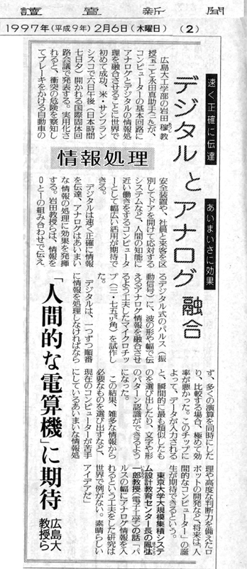
アナデジ融合技術 (広島大学時代)
アナログ・デジタル融合の新しいコンピュータの基本回路を開発ISSCC'97(国際固体回路会議)で永田真助手が発表.
この発表に関して岩田穆は新聞やテレビで報道され、中国新聞1997.2.5の夕刊トップに掲載。
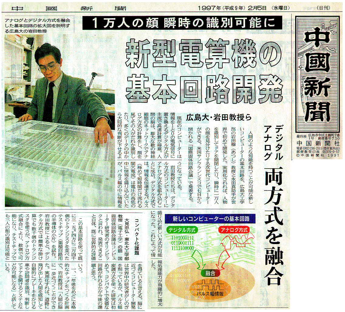
産経新聞1997.2.6 読売新聞1997.2.6
アナデジ混載LSIの雑音の解析と抑圧技術を開発 (広島大学時代)
CICC'97(カスタム集積回路会議)で永田真助手発表日経新聞記事2001.9.28
無線インタコネクション技術による三次元集積技術を開発 (広島大学時代)
中国新聞2005.2.9 日本経済新聞2005.2.9 産経新聞2005.2.9 毎日新聞2005.2.9
人材育成
人材育成の現場中国新聞2005.2.9 毎日新聞2005.2.9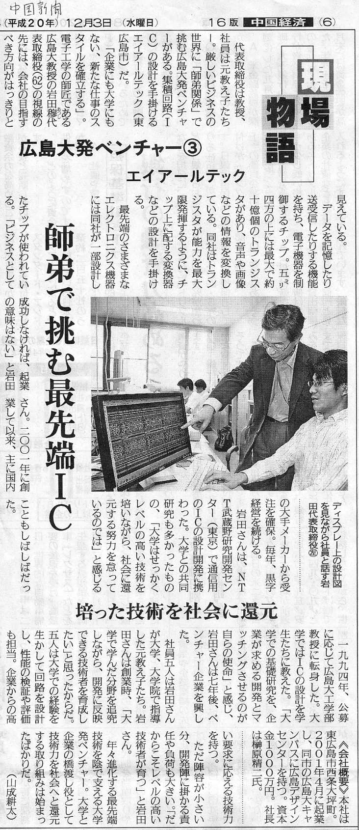
機能集積システム研究室(岩田穆研究室)
機能集積システム研究室の紹介記事がEngineer Colorsに開催された。(4ページ)
 p1:アナログデジタル混載から融合へ
 |
p2:無線三次元集積技術 > >
|
 p3:ナノデバイスによるバイオセンサー |
 p4:大学・企業の架け橋と人材御育成 |
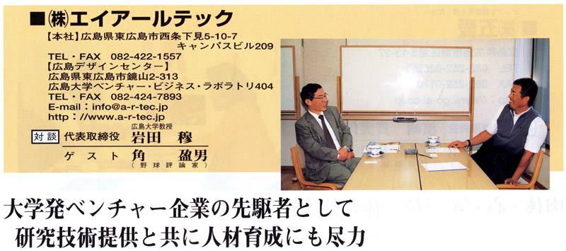
エイアールテックに関する報道
2001年に岩田穆はエイアールテック(A-R-Tec)を起業、「週刊東洋経済」や一般新聞各紙で報道された。
新聞各紙でも報道
日経新聞2001.4.7
中国新聞2001.4.7
読売新聞2001.4.7
毎日新聞2001.2.9
中国新聞2001.4.15
角さんのインタビューを受ける
国際画報
- 電子線走査装置およびその走査方法,第951391号,1979,(共同発明者:柴山, 藤波)
- RCアクティブフィルタ,第956412号,1979,(共同発明者:黒沢)
- 電子線偏向制御回路,第956564号,1979,(共同発明者:柴山,藤波)
- 荷 電粒子ビーム偏向制御方式,第965280号,1979,
- 分布RC素子を用いたアクテ ブ高域ろ波器,第979372号,1979,(共同発明者:黒沢)
- 電子ビーム偏向回路,第981750号,1979,(共同発明者:柴山)
- 電子ビーム直線走査信号発生方法およびその装置 ,第 984798号,1980,(共同発明者:柴山)
- 電子線描画装 置 ,第984808号,1980,(共同発明者:宇野)
- DA変換器,第989286号, 1980,(共同発明者:麻殖生)
- RCアクティブフィルタ ,第1040809号, 1981,(共同発明者:吉村)
- 電子ビーム走査位置補正方法,第1075992号, 1981,(共同発明者:藤波)
- トリミング装置,第1085655号,1982,(共同発 明者:小杉)
- ウエハ固定方法,第1107662号,1982,(共同発明者:藤波,石鍋)
- AGC回路,第1161607号,1983,(共同発明者:桜井)
- 復号化回路,第1257971号,1985,(共同発明者:菊池,内村)
- スイッチドキャパシタ 積分回路,第1270507号,1985,
- プログラマブルカウンタ,第1289270号, 1985,(共同発明者:菊池)
- AD変換回路,第1289282号,1985,(共同発明 者:菊池,内村,松谷)
- 整流検出回路,第1310955号,1986,(共同発明者: 橋爪)
- エンコーダ回路,第1358765号,1987,(共同発明者:鈴木,山内)
- エンコーダ回路,第1361311号,1987,(共同発明者:鈴木,山内)
- スイッチドキャパシタフィルタ,第1371324号,1987,(共同発明者:加藤,・纐・j
- スイッチドキャパシタフィルタ,第1371326号,1987,(共同発明者:加藤,上野)
- 積分回路,第1383652号,1987,(共同発明者:菊池,松谷,内村)
- スイッチドキャパシタフィルタ,第1395355号,1987,(共同発明者:上野,加 藤)
- ディジタルアナログ変換器,第1398950号,1987,(共同発明者:松谷, 赤沢)
- プログラマブルカウンタ,第1413150号,1987,(共同発明者:加藤, 菊池)
- 1次低域通過フィルタ ,第1419013号,1988,(共同発明者:金子, 内村,菊池)
- ディジタル並列加算器 ,第1426990号,1988,(共同発明者:守 谷,赤沢)
- 電圧分割回路,第1431751号,1988,(共同発明者:大畑,松村)
- 電圧分割回路,第1431751号,1988,(共同発明者:大畑)
- パルススワロ ー分周器,第1436767号,1988,(共同発明者:松浦,菊池)
- 半導体容量素子,第1443856号,1988,(共同発明者:小笠原)
- ダイナミックアナログ増幅器,第1452487号,1988,(共同発明者:内村)
- アナログディジタル変換器の自動補正方法,第1459681号,1988,(共同発明者:松谷,赤沢)
- 符号変換器,第1476332号,1989,(共同発明者:松村,後藤)
- ディジタルアナログ変 換器,第1480087号,1989,(共同発明者:松谷,赤沢)
- アナログディジタル 変換器,第1480088号,1989,(共同発明者:赤沢,松谷)
- 復号化回路,第 1483710号,1989,(共同発明者:梁川,岡本)
- 符号化回路 ,第1483711号, 1989,(共同発明者:梁川,岡本)
- アドレス制御回路,第1497207号,1989, (共同発明者:金子,山内)
- スイッチトキャパシタ回路,第1532415号, 1989,(共同発明者:内村)
- CMOS集積回路,第1533623号,1989,(共同 発明者:藤井)
- ディジタルアナログ変換器,第1541870号,197690,(共同発 明者:赤沢,松谷)
- 整流検出回路,第1549928号,1990,(共同発明者:橋爪)
- アドレス制御回路,第1592635号,1990,(共同発明者:金子,山内)
- スイッチドキャパシタフィルタ,第1610500号,1991,(共同発明者:上野)
- MOSアナログ信号増幅器,第1632986号,1992,(共・ッ・ュ明者:内村)
- アドレス制御回路,第1638477号,1992,(共同発明者:金子,山内)
- オーバーサンプリング形アナログディジタル変換器(MASH),第1639746号,1992,(共同発明者: 内村,小林)
- オーバーサンプリング形ディジタルアナログ変換器(MASH),第 1639747号,1992,(共同発明者:内村,小林)
- PLL回路,第1643159号, 1992,(共同発明者:伊藤)
- 基準電圧発生回路,第1643159号,1992,(共同 発明者:守,片岡)
- 位相同期回路,第1674360号,1992,(共同発明者:西 田,内村)
- 交流増幅回路,第1675545号,1992,(共同発明者:藤井)
- アレイプロセッサ,第1734856号,1993,(共同発明者:高橋,木村)
- アレイ プロセッサの制御方法 ,第1746672号,1993,(共同発明者:高橋,服部,木村)
- アンロック検出回路,第1755391号,1993,(共同発明者:r沢)
- スイッ チトキャパシタ回路,第1804944号,1993,(共同発明者:内村)
- 半導体容量 素子,第16995220号,1987,(共同発明者:小笠原)
- 周波数変調装置,特願平 6-118866号,1994(共同発明者:角山)
- 周波数変調信号復調装置 ,特願平 6-118888号,1994(共同発明者:角山)
- パルス変調演算回路 ,特願平9-22804号,1997,(共同発明者:永田)
- パルス幅変調演算回路 ,特願平9-22805号,1997,(共同発明者:永田)
- 2次元情報処理装置 ,特願平9-78025号,1997,(共同発明者:永田)
- 低スイッチ ング雑音論理回路,特願平10-203523号,1998,(共同発明者:永田,土方)
- アダマール変換回路 特願2000-259990号(片山,森江,永田)
- 半導体集積回路における電源電流波形の解析方法及び解析装置,特願2001-26795号,特許3569681 号(永田真),
- 集積回路基板の電位の解析方法および装置 特願2001-177830 2002.6.12 開2002-368116,(村坂佳隆,永田真)
- プログラマブルA/D変換器 特願2001-309280 開2003-115763(山口、森江,永田)
- 画像情報処理装置 特願2002-13464, 特開2003-219279 (今村,森江)
- 画像の直交変換回路 特願2002-262316,(2002.9.9),(片山,岩田)
- マッチングプロセッサ 特願2002-307455, (山本)
- マッチングプロセッサ 特願2002-307479, (山本)
- マッチングプロセッサ 特願2002-307739,(山本)
- デジタル情報処理回路プログ,特願2002-3340091,特許3973545号,2007.6.23
- プログラマブルアナログ・デジタル変換器,特許3717886号,2005.9.9,特願2002-367136,(山口,森,河部本,西田)
- 半導体装置,特願2003-117826,(2003.4.23),(吉川,角南,マタウシュ,横山,芝原,中島,小出,ラシド,渡辺)
- アナログディジタル変換回路,特願2004-2449,(2004.01.07),(吉田毅,佐々木守,赤木美穂)
- 半導体装置,特願2004-10053,(2004.01.19) 特開2005-203657 (佐々木守,有薗大介)
- 画像処理装置,特願2004-022317 (2004.1.28) 特開2005-217804,(亀田,佐々木,吉川)
- PWM伝送 特願2005-061703 2005.3.7 (今村,村坂)
- 信号伝達装置および信号伝達方法, 特願2005-147216, H17.5.19, (佐々木、有薗)
- 信号伝達方法, 特願2005-147227, H17.5.19, (佐々木、有薗)
- 半導体記憶装置, 特願2005-152077, H17.5.27, (池田、佐々木)
- アナログディジタル変換回路, 特願2004-342508, H16.11.26, (吉田、佐々木、赤木、後藤)
- AB級CMOS出力回路,特願2004-342421, H16.11.26, (吉田、佐々木、後藤)
- チョッパ増幅回路,特願2005-093683, H17.3.29,(吉田毅、佐々木、真下、升井、中塚).
- インダクタ対の磁気結合を利用したシリアルデータ伝送装置, 特願 2006-293338,H18.1.27, (飯塚,閻,佐々木)
- デルタシグマAD変換器,特願2010-117959, H22.5.24,(村坂,今村,岩田)